



Electronic Materials
Electronic Materials
For cutting-edge electronic devices, we offer distinctive semiconductor materials, conductive materials, and magnetic materials using technologies such as ultra-purification, single crystal and thin film growth, and particle synthesis.
Core Technologies
Crystallization Technology
-
- High-Purity and Analytical Technology
-
- We have a variety of high-purification technologies of 6N (99.9999%) or more, as well as analytical technologies that can handle impurities on the order of ppb.
-
- Single Crystal Growth
-
- We have low-defect single crystal growth technology by controlling composition and temperature.
- We have wafer surface purification, flatness and surface treatment technology.
- We have the technology to increase the diameter of wafers.
-
- Single Crystal Thin Film Growth
-
- We have a variety of III-V compound semiconductor thin film growth technologies.
- Optimal design achieves both optical characteristics and low electrical resistance.
- We have the technology to grow a uniform single crystal thin film by controlling the composition and temperature.
-
- Semiconductor Design & Manufacturing Technology
-
- We have built an integrated system from raw materials to high-purity metals, single crystal substrates, epitaxial substrates, and devices.
- Optimal design achieves both optical characteristics and low electrical resistance.
- We use MES (Manufacturing Execution System) for process management.
-
- Evaluation and Analysis Technology
-
- We have epitaxial substrate evaluation technology and automatic device inspection technology (electro-optical characteristics and appearance).
Powder Control Technology
-
- Wet Synthesis
-
- We have the following synthesis technologies for magnetic powders, metal powders (Ag, Cu, alloys), and oxide powders.
-
- Particle size can be controlled from several nanometers to several micrometers.
- Particle shape can be controlled into spherical, needle, flake, etc.
- Particle size distribution and metal composition can be controlled.
-
- Dry Synthesis
-
- We have the following synthesis technologies for magnetic powders, metal powders (Ag, Cu, alloys), and oxide powders.
-
- Particle size can be controlled from submicron to several tens of micrometers.
- Particle size distribution and metal composition can be controlled.
-
- Powder Processing
-
- We have the following powder processing technologies for magnetic powders, metal powders (Ag, Cu, alloys), and oxide powders.
-
- Shape control technology (flakes)
- Particle size distribution control technology by advanced classification
- Crystal structure control technology by firing
-
- Surface Control
-
- We have the following surface control technologies for magnetic powders, metal powders (Ag, Cu, alloys), and oxide powders.
-
- Conductive material coating
- Non-magnetic layer coating
- Withstand voltage coating
-
- Conductivity Control
-
- Wet synthesis, dry synthesis, powder processing, and surface control can provide the following conductive materials to meet your needs:
-
- Chemically reduced Cu powder
- Atomized Cu powder, Atomized Ag powder
- Flake-type Cu powder
- Nano-size Ag powder
- Oxide coated active material powder
-
- Magnetic Control
-
- Wet synthesis, dry synthesis, powder processing, and surface control can provide you with the following magnetic materials to meet your needs:
-
- Ferrite powder, carrier powder
- Silica coated soft magnetic powder
-
- Mass Production Design
-
- We have scale-up technology that covers from research to mass production.
- We own facilities capable of supplying products up to several hundred tons per month.
Examples of Core Technology Applications
-
- High-Purity Technology and Analytical Technology
-
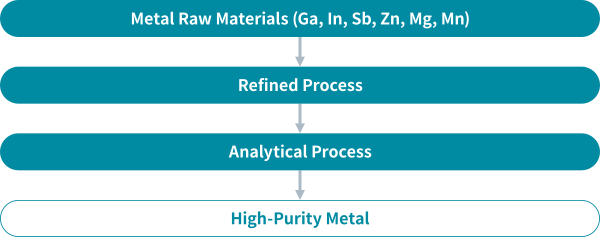
- Manufacturing Flow (example)
-
-
- Features of Technology (Our Strengths)
-
- By making full use of a variety of purification technologies (crystal purification, electrolytic purification, distillation purification, vacuum purification), it is possible to achieve high purity of 99.9999% or more.
- We have advanced impurity analysis technology that enables impurity analysis on the order of ppb.
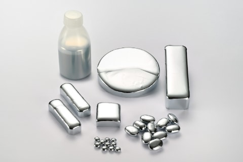
High-Purity Metal
-
- Single Crystal Growth Technology
-
- Manufacturing Flow (example)
-

-
- Features of Technology (Our Strengths)
-
- We have a variety of crystal growth technologies such as the LEC method and the VGF method.
- Highly accurate carrier density control is possible.
- Single crystals with low EPD (Etch pit density) can be obtained.

GaAs Single Crystal Substrate
-
- Thin-Film Single Crystal Growth Technology
-
- Manufacturing Flow (example)
-

-
- Features of Technology (Our Strengths)
-
- We have high-quality III-V group compound semiconductor thin film (AlGaIn-AsPSb, AlGaIn-N) growth technology using LPE method and MOCVD method.
- We have high-precision impurity concentration control technology and film thickness control technology.
- Compatible with a wide variety of substrate sizes
- We own evaluation equipment such as PL (Photoluminescence) equipment, XRD equipment, ECV equipment, Hall effect measurement equipment, non-contact sheet resistance measurement equipment, wafer surface inspection equipment, AFM (Atomic Force Microscopy), SEM and other evaluation equipment.

Epitaxial Substrate
-
- Semiconductor Design and Manufacturing Technology
-
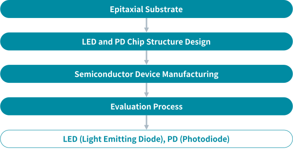
- Manufacturing Flow (example)
-
-
- Features of Technology (Our Strengths)
-
- We have LED high-output technology by surface treatment.
- We have technology to improve the optical characteristics of LEDs by forming optimal electrodes and reduce resistance.
- LED output, wavelength, and shape can be customized.
- We have technology to automatically inspect electro-optical properties and appearance.

LED 
Photodiode
-
- Powder Processing Technology Wet Manufacturing
-
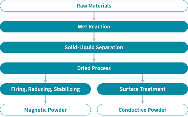
- Manufacturing Flow (example)
-
-
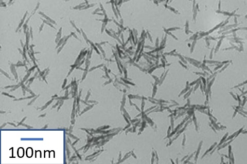
Magnetic Powder (FeCo) -
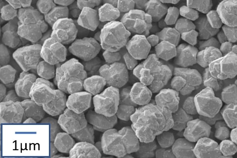
Conductive Powder (Copper
Powder 1.5 micrometers) -
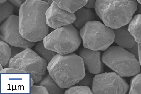
Conductive Powder (Copper
Powder 3.0 micrometers)
-
-
- Features of Technology (Our Strengths)
-
- There are technologies to control nucleation and growth in wet particle synthesis.
- We can be possible to control the particle size, shape, particle size distribution, composition, and surface of nano- and micron-sized powders.
-
- Powder Processing Technology Dry Manufacturing
-
- Manufacturing Flow (example)
-

-

Atomized Copper Powder -

Atomized Silver Powder -

Gas Atomized Metal Powder
-
-
- Features of Technology (Our Strengths)
-
- We can provide various kinds of metals (copper, silver) and alloy powders.
- Composition and particle size can be controlled from submicron to several tens of microns.
-
- Powder Processing Technology: Flakes, Surface Treatment
-
- Manufacturing Flow (example)
-
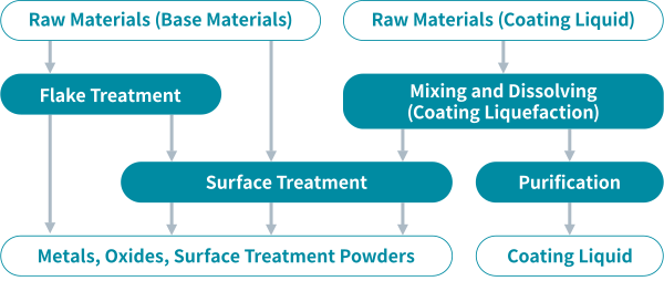
-

Atomized Flakes Copper Powder -
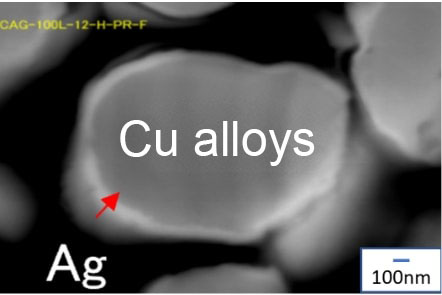
Silver Coated Copper Powder -
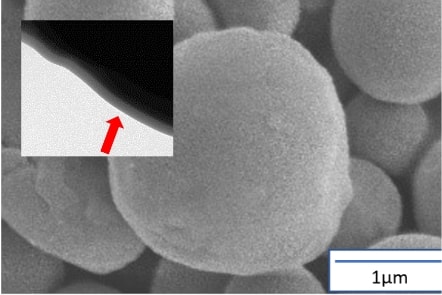
SiO2 Coated Soft Magnetic Powder -
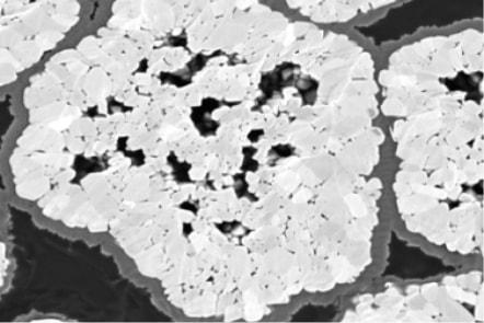
Oxide Coated Active Material Powder
-
-
- Features of Technology (Our Strengths)
-
- We can control the shape and surface of particles.
- We can provide silver-coated copper powder as an alternative to silver.
- We offer SiO2 coated soft magnetic powder with surface treatment (SiO2 coating) for high heat resistance and insulation.
- We are improving the conductivity and durability of active material powder for use as rechargeable battery materials.