Our Strengths
Advanced Manufacturing Facilities
Our facilities are designed not only to strengthen QCD but also to consider the protection of the local environment and the safety and comfort of employees.
New Building (Building P)
Completion of the New Building scheduled for 2023
We have begun construction of a new building (Building P).It is designed with environmental considerations, including solar panels and energy-saving air conditioning systems.
Vertical Warehouse
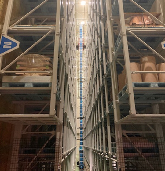
In addition to facilitating space-saving storage and optimizing storage conditions through air conditioning and the like, it contributes to the efficiency of in-house logistics and the reduction of employee workloads.
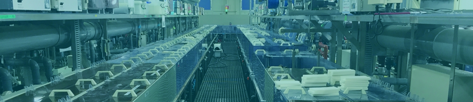
Integrated Plating Line for Multiple Plating Types
This plating line enables to process silver (Ag) and tin plating (Sn), which were formally done in separate processes, in a consistent manner. It can reduce lead times (quick delivery) and improve efficiency in production management.
Bio Palette
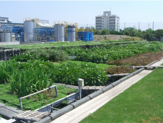
Within the premises of DOWA HIGHTECH, we have installed an environmentally friendly water purification facility called "Bio Palette," which utilizes the purification capabilities of microorganisms and insects in natural ecosystems.
The plant-treated wastewater passes through the ecosystem created inside the Bio Palette, resulting in further purification of the water.
Active Utilization of Digital Technology
Our company actively employs digital technology to build superior operational management systems and quality assurance systems.
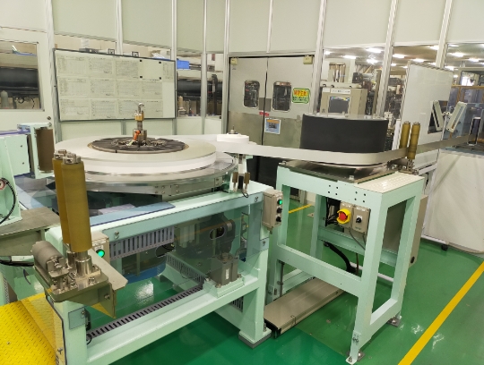
We have implemented image processing equipment in all plating lines to check the entire length of the coils. We manage operational conditions and history through a database, and this enables real-time confirmation.
Plating technical expertise.
At our company, we conduct various technological developments related to the plating business, such as developing plating films and improving plating processing technologies, based on the needs of our customers.
We have placed a dedicated technology development team inside DOWA HIGHTECH Co., Ltd., our manufacturing base, to establish an integrated development system that unites research and manufacturing.
Additionally, we own facilities dedicated to technology development, such as specialized plating lines, allowing us to carry out advanced and efficient technological development.
Global Expansion
Our company is expanding its business from our mother factory, DOWA HIGHTECH Co., Ltd. (located in Honjo City, Saitama Prefecture), with two locations in Thailand and one in Mexico, totaling four bases. Since all of our bases, both domestic and international, adhere to the same technical standards and set processing conditions accordingly, we can guarantee consistent quality.
Additionally, our overseas locations are capable of plating on local materials, allowing us to flexibly meet a variety of requirements for localization.
Part of the DOWA Group
We are a member of the DOWA Group, which has its foundation in mining and smelting business. We collaborate with various companies within the group to meet a wide range of customer needs.
As an example, we would like to introduce our collaboration with DOWA Technology.
DOWA Technology Kanto Technical Center is located on the same premises as DOWA HIGHTECH. The Kanto Technical Center owns a wide range of analysis equipment, enabling various analyses tailored to customer needs.
List of Surface Analysis Instruments
| Analysis Instrument | Target | Performance | |
|---|---|---|---|
| Surface Analysis | FE-SEM+EDS | Surface roughness, size, and shape of solid, powder and metal. | 20-40,000x magnification with a resolution of 1.0mm (acceleration voltage of 15kV). |
| FIB | Fine cross-sections of powders, crystals, metals | SIM Imaging: 150-30,000x | |
| TEM+EDS | High-resolution transmission electron microscopy of solid, powder, metal | Several thousand-1.5 million x, Point resolution: 0.23 nm | |
| SPM | Surface roughness and shape of solids | DFM, AFM measurements, non-contact measurements | |
| FE-AES+EBSD | Surface and depth direction element analysis of solid, powder and metal | Up to 50,000x, Practical:>0.1% | |
| EPMA+EDS | State of element existence in [Solid, Powder, Metal] | 40-10,000x, Secondary electron image resolution: 6 nm (WD: 11 mm, 30 kV) | |
| XPS | Surface condition of solid, powder and metal | Depth of several tens of angstroms with a minimum analysis area of 10 μm. | |
| FT-IR | Identification of solids | Microscopic measurement starting from 20 µm in diameter. | |
| Chemical Analysis | ICP-OES | Metal components in solution | Solution: 0.1 mg/L+, Solid: 10 ppm - |
| ICP-MS | Metal components in solution | Solution: 0.01 mg/L+, Solid: 1 ppm - | |
| IC | Ion components in solution | 0.1 mg/L - | |
| LC-MS/MS | Hydrophilic organic compounds | 0.001 mg/L - | |
| GC/MS | Volatile organic compounds | 0.1 mg/L - | |
| ONH Analyzer | Solids that melt or decompose at high temperatures | 50 ppm - 5% | |
| UV/VIS | Ultraviolet absorption or colored liquids | 50 ppm - 5% | |
| XRF | Qualitative analysis of solid samples | 1% - | |
| XRD | Powders | 1% - | |
| TG-DTA | Powders | TG measurement range: ±400 mg, DTA measurement range: ±1000 μVc |